- News
12 October 2011
Integrating electrostatic discharge handling into nitride LEDs
Researchers in China have increased the resilience of nitride semiconductor light emitting diodes under negative bias from -1200V to -4000V by using four layers of silicon delta-doped (Si DD) material as part of the n-cladding [Zhiyuan Zheng et al, Appl. Phys. Lett., vol99, p111109, 2011]. It is thought that the improvement is due to better current spreading across the device and material quality enhancement. The research was carried out at State Key Laboratory of Optoelectronic Materials and Technologies, Sun Yat-sen University, Guangzhou.
The LED samples were grown on c-plane sapphire using metal-organic chemical vapor deposition. The active region consisted of a 6-period multi-quantum well (MQW) of indium gallium nitride (In0.17Ga0.83N) separated by GaN barriers. A standard device was produced with a 2.3μm-thick heavily Si-doped n-cladding layer (carrier density 6x10¹⁸/cm3), and 200nm magnesium-doped p-GaN layer.
A second device with four Si delta-doped (Si-DD) layers separated with 50nm of GaN between the MQW and n-cladding layers were also produced. The n-cladding was reduced in thickness in the second device to 2.1μm to maintain the same total thickness of the n-type layer between the devices. The delta doping was achieved by alternatively switching the trimethyl-gallium and silane (SiH4) sources on or off, while maintain the ammonia (NH3) flow.
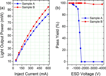
 Mesa structure 1x1mm LEDs were produced from the epitaxial samples. The output power (Figure 1a) of the device with delta-doped n-GaN (sample B) was 64.8mW at 350mA, 12.8% higher than that of the standard device (sample A). Since the sapphire substrate is insulating, the electrode contacting with the n-type material of the device is off to the side of the device. This means that the electron current has to flow laterally under the active region before they can ascend to the active region.
Figure 1: (a) Light output power and (b) ESD properties of devices without and with Si delta-doping layers (samples A and B, respectively).
The electrostatic discharge performance (Figure 1b) was assessed by applying negative biases up to -4000V and then testing the reverse bias leakage current at -5V. If the leakage current exceeded 5μA, the device was considered to fail the test. With this criterion, device A failed at -1200V, but
LED-B continued to pass at -4000V. The measurements were made on an IPT 6000 Fit Tech system with a human-body-mode ESD module.
The researchers also wanted to know why their delta-doping technique improved ESD handling by investigating possible explanations such as capacitance modulation, better current spreading and improved material quality. However, the researchers found “no obvious discrepancy” between their devices A and B in terms of capacitance-voltage performance, so they rejected capacitance modulation as the origin of improved ESD performance.
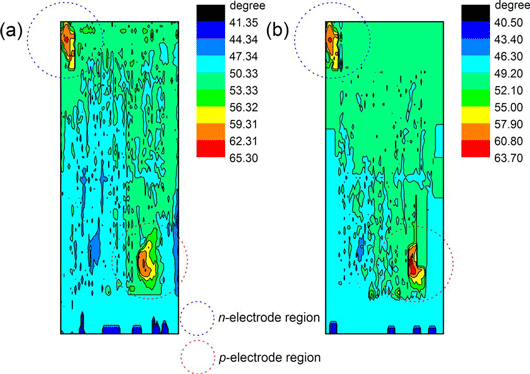
The researchers looked next at the thermal properties of the devices using infrared microscopy (Figure 2), seeing a more uniform distribution in LED-B that would indicate better current spreading. “We ascribed this improvement to the enhanced electrical conductivity of the Si-DD layers,” write the researchers. Hall measurements on the normal (A) and Si-DD (B) n-cladding structures gave mobilities of 180cm2/V-s and 218cm2/V-s, respectively. This would give a 17% increase in conductivity for LED-B, enhancing current spreading under the active region and thus lowering the current density across the device. These factors would improve ESD performance.

Figure 2: IR camera images of (a) sample A and (b) sample B driven by 350mA injection current.
Current spreading could also improve light output power through reducing the droop effects of high current density (see, for example, Current spreading for higher nitride LED output power).
Current-voltage measurements show little difference between the devices in forward bias, but in reverse bias, leakage currents are typically reduced more than one order of magnitude (factor of 10) in LED-B: at -5V, the current in LED-A is 8x10⁻⁷A, compared with 4x10⁻⁸A for LED-B. The researchers suggest that the improvement in LED-B could be due to reduced dislocation density in LED-B. It is thought that Si-DD can reduce screw-type dislocations by an annihilation effect. Another possibility that may be operating is blocking of pure edge dislocation propagation through formation of silicon nitride complexes.
High threading dislocation densities are created in growth of nitride semiconductors on sapphire due to the large lattice mismatch (~14%) and differences in thermal expansion between the materials.
X-ray diffraction patterns were little different between the devices - LED-B did have a slightly narrower rocking curve, but not enough to validate improved material quality. The peak intensity in photoluminescence experiments for LED-B was about double that of LED-A. The peak occurred at 470nm wavelength. The much higher emission peak intensity suggests improved quality of the epilayers in the DD structure.
Wet chemical etching suggests also reduced dislocation density with a density of etch pits of 7x10⁷/cm2 for epitaxial sample A and 3x10⁶/cm2 for B. The hexagonal pyramid shape of the pits indicated that the dislocations were mixed- and screw-type. Lowering dislocation densities reduces current leakage paths, enhancing ESD handling and increasing light output.
The author Mike Cooke is a freelance technology journalist who has worked in the semiconductor and advanced technology sectors since 1997.
