- News
11 May 2011
Nitride HEMTs with 245GHz cut-off
Researchers based in the USA have produced gallium nitride (GaN) semiconductor high-electron-mobility transistors (HEMTs) with indium aluminum nitride (InAlN) barriers that achieve cut-off frequencies (fT) of 245GHz [Dong Seup Lee et al, IEEE Electron Device Letters, published online 29 April, 2011].
The scientists from Massachusetts Institute of Technology, IQE RF LLC and University of Notre Dame thus claim “the highest fT ever reported in GaN transistors”. They add: “These results demonstrate the great potential of InAlN/GaN HEMTs for millimeter- and submillimeter-wave applications.”
The record performance was achieved thanks to an oxygen (O2) plasma treatment that reduces gate leakage currents by more than two orders of magnitude. “In addition, the RF transconductance (gm) collapse is reduced in the O2-treated devices, which results in a significant improvement in the fT,” the researchers say.
The epitaxial structures for the HEMTs were grown on silicon carbide substrates using metal-organic chemical vapor deposition (MOCVD). The 45Å barrier layer of In0.17Al0.83N was lattice matched with the underlying GaN buffer layer with a very thin 10Å AlN interlayer. Hall measurements on this epitaxial material gave a two-dimensional electron density of 1.5x10¹³/cm2 with a mobility of 1670cm2/V-s and sheet resistance 250Ω/square.
The use of lattice-matched material promises improved device reliability behavior long term, compared with the more usual GaN HEMTs with aluminum gallium nitride (AlGaN) barriers. A further attractive feature is a strong spontaneous polarization field in InAlN, inducing a high sheet charge density even with barriers thinner than 10nm.
Very thin barriers are needed to avoid complicated gate recessing etch processes where the barrier is thinned in the gate region to bring the electrode closer to the channel. Such recessing requires increasing etch accuracy as devices are scaled to the smaller dimensions needed for high-frequency performance. Nitride semiconductor technologists also avoid etch processes where possible, due to their potential to damage device performance.
Device fabrication from the InAlN/GaN/SiC epitaxial material consisted of mesa isolation, deposition of titanium-aluminum-nickel-gold ohmic source–drain contacts, and annealing at 850°C for 30 seconds in nitrogen.
The gate deposition process was begun with the oxygen plasma treatment and then electron-beam lithography to define a rectangular gate opening on the oxidized layer. The gate electrode consisted of nickel-gold. The access region of the device was cleared of oxide with a buffered etch.
The device was passivated with aluminum oxide (Al2O3) using atomic layer deposition (ALD). The produced HEMTs had gate lengths as short as 30nm.
The researchers comment: “It should be noted that this fabrication technology results in very short gate-length devices but high gate resistance. Although the high gate resistance will not allow the practical use of these devices in RF applications, the simple gate geometry allows the careful study of the frequency limitations of InAlN/GaN transistors.”
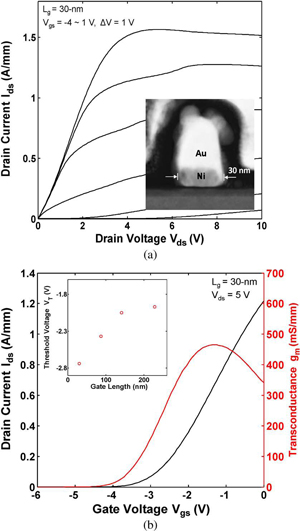
 Figure 1 (right): (a) Current–voltage (I–V) characteristics of an InAlN/GaN HEMT (gate length 30nm and width 50μm). Inset: transmission electron micrograph of 30nm-long gate. (b) Corresponding transfer curve at drain bias 5V. Inset: threshold voltage change depending on gate length. DC measurements were conducted by using one finger of device.
The DC characteristics (Figure 1) of the 30nm device include a maximum drain current of 1.57A/mm at a gate potential of 1V, and peak extrinsic transconductance (gm) of 467mS/mm. The transconductance value was affected by unoptimized contacts and short-channel effects. The gm value of a device with 140nm gate length produced on the same wafer was 509mS/mm.
The research team comments: “Even with the thin barrier thickness (45 + 10Å), the short-channel effects cannot be ignored as the gate length decreases below about 50nm.”
A further short-channel effect was a decrease in the threshold voltage with gate lengths less than 100nm (inset Figure 1). “A thinner barrier or the use of InGaN or AlGaN back barriers is necessary to completely suppress short-channel effects in highly scaled devices with sub-50nm gate lengths,” the researchers say.
RF measurements, leading to the cut-off frequency of 245GHz (250GHz according to Gummel’s method), give a very poor maximum oscillation frequency (fMAX) of only 13GHz due to the high resistance of the rectangular gate structure. The researchers believe that significantly improved results would result from use of mushroom-shaped gate structures or multi-finger devices with rectangular gates. They warn, “It is important, however, to carefully design them to minimize their parasitic capacitances and the potential degradation in fT.”
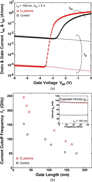
 Figure 2 (right): Effects of oxygen plasma treatment on (a) DC and (b) RF characteristics in InAlN/GaN HEMTs. Inset: intrinsic RF gm at bias point of maximum fT.
The researchers also compared performance of devices with and without oxygen plasma treatment (Figure 2). The main difference found is a suppression of gate leakage current by more than two orders of magnitude in devices with the oxygen plasma treatment. This effect is attributed to the insulating effect of the thin oxide layer resulting from the plasma exposure. Another effect of the oxide layer is a slight decrease in the threshold voltage due to the increased distance between the gate and the channel. Neither the mobility nor the sheet resistance are affected by plasma treatment.
The researchers also carried out small-signal equivalent circuit analysis, finding that the fT improvement is due mainly to the higher RF peak transconductance of the plasma-treated devices. The exact mechanism for this reduced transconductance collapse at high frequency “is still under investigation”.
The MIT/IQE/Notre Dame work received financial support from Defense Advanced Research Projects Agency (DARPA) Nitride Electronic NeXt-Generation Technology (NEXT), Office of Naval Research (ONR) Defense University Research Instrumentation Program (DURIP), and NSF CAREER Award.
Back-barrier to InAlN HEMT short-channel effects
GaN HEMTs InAlN/GaN HEMTs MOCVD IQE
http://dx.doi.org/10.1109/LED.2011.2132751
The author Mike Cooke is a freelance technology journalist who has worked in the semiconductor and advanced technology sectors since 1997.
