- News
14 March 2011
Superabrasives supplier Engis to double size of HQ
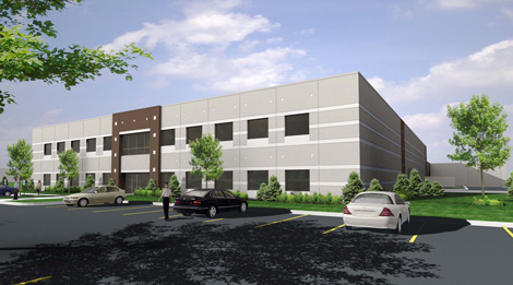
Engis Corp, which provides superabrasive finishing products and fully configured, custom-developed manufacturing systems for lapping, honing, polishing and grinding, plans an expansion that will nearly double the size of its world headquarters in Chicago suburb Wheeling, IL, USA, expanding its manufacturing and warehouse facilities and creating space for the new Engis Technology Center.

Picture: Architectural rendering of Engis expansion.
Engis supplies ‘HYPREZ’ high-precision micronized diamond, cubic boron nitride (CBN) powders, slurries, compounds, grinding wheels, machine tools and accessories. The privately held firm says that its ‘systems approach’ combines product and process knowledge to develop complete solutions to improve part quality, lower cost and reduce cycle times. Engis employs about 140 people in Illinois and 200 worldwide, including five locations in Asia, one in Europe and one in Canada.
The 54,000ft2, multi-million-dollar expansion will more than double total space to 121,500ft2 and enable the firm to consolidate all engineering, process development labs, manufacturing, warehousing and administrative offices into a single facility. In conjunction, Engis will add new manufacturing, process development and testing and measurement equipment. Construction will start in April and be complete by fall 2011.
“New automated manufacturing equipment will enable us to increase our ability to support global markets, while the Engis Technology Center will enhance our capability to develop turnkey manufacturing solutions,” says president Stephen Griffin. “It also demonstrates our commitment to keep and generate future jobs in Wheeling and in the USA,” he adds.
The cornerstone of the expansion will be the new Engis Technology Center, where the firm will work with customers to finish components to nanometer tolerances and achieve mirror surfaces. The center will house five labs:
- The Wafer Process Lab (WPL), which serves the advanced material and compound semiconductor markets.
- The Process Development Lab (PDL), which provides assistance for general industrial lapping and polishing inquires;
- The Hard Disk Drive (HDD) Lab, which focuses on the data storage industry.
- The Diamond Characterization Lab (DCL), which also includes the Engis’ Metrology (measurement) Lab.
- The Bore Finishing Lab (BFL), which works with customers on honing and bore finishing applications in the automotive, hydraulic, medical, advanced ceramic, compressor, aerospace and defense industries.
“Consolidating all the labs in one location will enable us to concentrate our engineering resources and enhance our customer service activities,” says Griffin.
Engis currently leases space for some of its process labs and other activities at a nearby location. All of these operations will be incorporated into the new expansion.
Join Semiconductor Today's LinkedIn networking and discussion group
