- News
23 June 2011
Kyoto makes record current-gain SiC BJTs
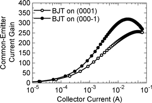
Kyoto University has produced silicon carbide (SiC) bipolar junction transistors (BJTs) with record current gains that have more than doubled previous achievements using the 4H polytype crystal structure [Hiroki Miyake et al, IEEE Electron Device Letters, published online 7 June 2011]. By reversing the polarity of the structure (000-1) to give a carbon face, the scientists created a device with a gain of 335, which is the highest value for BJTs built using any SiC polytype. Using the traditional Si-face (0001), the gain of 257 was almost double the previous best for 4H-SiC of 134.
The Kyoto researchers are developing the devices with power applications in mind, where high breakdown voltages and low on-resistance can be achieved. Also, BJTs do not suffer from the gate oxide reliability issues of MOSFETs resulting from high-temperature operation.
To improve the device performance, Kyoto focused on reducing surface recombination currents on the emitter mesa sidewall and increasing carrier lifetimes in the p-SiC base region of the BJT by reducing the number of deep levels in the material. Deep levels encourage the recombination of carriers through the Shockley–Read–Hall mechanism.
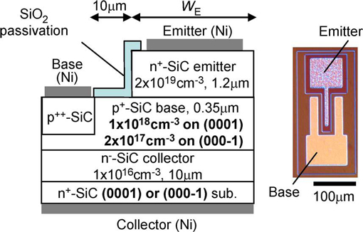
Two types of BJT were grown on n-type 4H-SiC substrates oriented with (0001) Si face and (000-1) C face using chemical vapor deposition (Figure 1). The surface was mis-oriented by 8° in the [11-20] direction. Such mis-orientation is frequently used to improve growth quality since the effect of mis-cutting the surface is to create a series of steps for new material to attach to as deposition proceeds. Mis-cutting has also been found to affect surface recombination at mesa sidewalls.

Figure 1: Schematic cross section of a fabricated 4H-SiC BJT and optical image of a fabricated single-finger BJT.
The p-type base layer was achieved using aluminium doping, while the n-type emitter layers were created using nitrogen doping. The heavily p-type base contact was formed using aluminium ion implantation at 500°C to create an Al concentration of 3x10²⁰/cm3.
Two 1150°C thermal oxidation processes were carried out before and after the annealing process for the base contact activation (1800°C for 10 minutes). To get the same oxide thickness required 5 hours on the (0001) devices and only 15 minutes on the (000-1) devices.
The purpose of the oxidation process is to reduce the major deep levels often labeled as Z1/2 and EH6/7, associated by some researchers with such defects as Si/C di-vacancies and carbon vacancies that form charge traps.
Although the oxidation treatment does reduce these levels, it generates the HK0 center/level that is also seen with carbon tetrafluoride (CF4) reactive ion etch (RIE). However, the HK0 center/level anneals out at 1550°C, so the activation process removes it, but then reintroduces Z1/2 and EH6/7 levels, giving the need for the second oxidation.
Surface levels were handled with a passivation process that involved a nitrided oxide deposition using a 10% dilute nitric oxide (NO) treatment at 1300°C for 30 minutes.
The single emitter finger contact was 100μm long, deposited in different crystal directions with {11-20} or {1-100} sidewalls to vary the effect of surface recombination. Emitter–base contact separation was 10μm.
For the achievement of a high current gain of 257 with a Si (0001) face structure, {1-100} sidewalls, and 20μm finger width, it was found to be important to grow the heterostructure in a continuous process in a single reactor. A comparison device with the base and emitter layers grown in separate runs had a current gain of around 80.
Since the Kyoto heterostructure is almost the same as that of these previous devices, the researchers “assume that not only continuous growth but also well-optimized surface passivation combined with an intentional deep-level-reduction process described in this letter contributed to such high current gains.”
Wider fingers with {1-100} sidewalls have higher current gain due to reduced surface recombination compared with {11-20} sidewalls (242 gain). The improvement for wider fingers saturates at widths beyond 20μm.
 The BJTs on C(000-1) face substrates demonstrate the even higher gains of 335, which the researchers say is the highest value ever reported for SiC BJTs (Figure 2). The peak occurs for a lower collector current because the doping concentration of the base layer for the C(000-1) face device is a factor of five smaller than that for the Si(0001) face BJTs.
Figure 2: Current gains as a function of collector current for BJTs with 20μm-wide fingers and {1-100} sidewalls fabricated on (0001) and (000-1).
The researchers comment: “It should be noted that we applied the surface passivation process and DLR-process optimized for SiC (0001); thus, there is still room for improvement in the fabrication processes. However, the operation of C-face BJTs with such high current gain described in this letter indicates the future possibility of C-face BJTs.”
The author Mike Cooke is a freelance technology journalist who has worked in the semiconductor and advanced technology sectors since 1997.
