- News
22 June 2011
University of Warsaw installs FIB milling system to create micropillars
Focused ion beam (FIB) milling equipment from FEI Company installed at the Faculty of Physics, University of Warsaw (FUW) has made it possible to produce micropillars semiconductor structures that can be used as efficient light sources.
“Being able to generate micropillars directly in the university laboratories is of key importance to our research, especially as regards works on really efficient yellow laser light sources,” says Wojciech Pacuski PhD. The equipment purchased by the Institute of Experimental Physics FUW is one of only a handful of such devices in Poland.
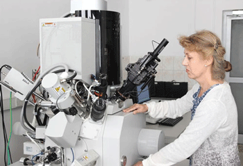
 Picture: University of Warsaw’s Jolanta Borysiuk during venting of the focused gallium ion beam milling equipment.
Micropillars are a type of optical microcavity structure in which photons are confined for a relatively long time in a small volume. Micropillars are obtained by milling a surface that was previously constructed out of many nanoscale-thick layers of semiconducting materials with carefully selected characteristics. “The surfaces out of which we are currently fabricating micropillars were made at the University in Bremen. Soon, we will be able to make them here as well with the aid of another acquisition of the Faculty, currently being installed – molecular beam epitaxy (MBE) equipment,” says Tomasz Jakubczyk, a PhD student at the Solid State Physics Division of the Institute of Experimental Physics FUW.
To fabricate a micropillar, researchers need to remove material from the surface with precision, in such a way as to create a pillar with a diameter and height of the order of microns. The Helios NanoLab system, which allows milling of a surface with a beam of gallium ions, is hence used. After being accelerated to high energy, ions are focused to an accuracy of several nanometers and directed towards selected points on the surface. Given their considerable size and mass, the gallium ions do not penetrate inside the material, but rather sputter atoms from its surface. The sputtered atoms disperse in the vacuum chamber. The effects can be assessed immediately by a scanning electron microscope (SEM), which is an integral part of the system. Apart from micropillars, it is also possible to generate other dimensional semiconductor structures using this method.
The focused ion beam milling equipment (worth 5 million zlotys) was purchased as part of the Centre for Preclinical Research and Technology project, co-financed under the European Regional Development Fund as part of the Operational Programme Innovative Economy 2007–2013. “The equipment will be available not only to researchers, but also to students from the Faculty of Physics UW specializing in condensed-matter physics, including those who pursue the recently introduced nanostructure engineering interdisciplinary studies,” stresses Pacuski.

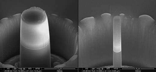
Picture: Electron microscope image of the first micropillars fabricated at the Faculty of Physics, University of Warsaw.
The University of Warsaw says that micropillars have many applications, especially in constructing single-photon sources and generating entangled photon pairs. Sources of this type are used, among others, in work on optical and quantum computers and in quantum cryptography.
Researchers in the Faculty of Physics are particularly interested in micropillars containing quantum dots. “Quantum dots themselves are good sources of single, and even entangled photons, but the desired characteristics are additionally enhanced when they are placed inside micropillars,” says Jakubczyk. “A micropillar with quantum dots can, for example, emit single photons more frequently,” he adds.
Physicists at the University of Warsaw aim to use the new equipment to construct micropillars that are sources of yellow laser radiation. “With a method devised by Pacuski PhD, in collaboration with colleagues from Bremen and patented in 2009, we can create mirrors, which are a crucial element of a laser, on both ends of micropillars,” says Jakubczyk. “The fact that we are one of a handful of laboratories in the world specializing in materials from the II and VI group of the periodic table is an additional asset in works on a yellow laser. These compounds emit light precisely in the wavelength range corresponding to yellow light,” he adds.
Microlasers emitting yellow light will be fabricated as part of the ‘Lider’ project. The devices could be useful in telecom applications that use plastic optical fiber (POF), which attenuate yellow light the least. In addition, increasingly popular displays offering an additional range of colours (other than the standard RGB) also rely on yellow lasers.
Focused ion beam milling FEI Company MBE
