- News
7 July 2011
MHI’s µV1 machines SiC and sapphire wafer materials, eliminating photomasks
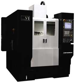
Tokyo-based machinery manufacturer Mitsubishi Heavy Industries Ltd (MHI) says that it has used its µV1 micro-milling system to machine four types of extremely hard, difficult-to-cut wafer materials: silicon carbide (SiC), sapphire, glassy carbon and silica glass.
 On the revised Mohs hardness scale, which rates the hardness of a diamond at 15, SiC is rated at 13, making it the third hardest wafer material, and sapphire is a 12, the fourth hardest. Glassy carbon is rated between 10 and 11 and silica glass is a 7.
The µV1 is able to create grooves and grids to micron-level accuracy on wafers using a cutting process only (i.e. without additional processes that are necessary when creating grooves and grids by photolithography or etching) enabling significant reductions in production time and cost, it is claimed. MHI aims to expand sales of the µV1 for trial machining of semiconductor materials and sample production.
For machining wafer materials, the µV1 uses a cutting tool made of diamond. To remove hard fine swarf mixed with coolant oil, the machine is equipped with a special fine swarf collection filter. MHI says that its proprietary Optical Image-type Tool Measurement System can accurately measure the position of the rotating tool end using a CCD (charge-coupled device) camera, enabling precise real-time monitoring of tool tip position. This feature allows the machine to obtain tool rotation dynamic accuracy data and to offset thermal displacement caused by the heat generated by the machine itself, ensuring precise cutting of grooves with micron-level accuracy.
The µV1 was released in 2006 as a three-axis milling machine for the machining of precise die and mold, electrodes as well as precision parts. In 2008, a five-axis model (which has table tilting function with rotary axes) was added to the series. To date, applications of the µV1 have been expanded to include machining of non-ferrous materials and the production of small-sized jigs.
When photolithography or etching is used for semiconductor shaping in trial or sample production (applications in which production quantities are inherently limited and production is subject to frequent changes) these methods tend to inflate costs, as they require the production of multiple masks for each modification in semiconductor shape, says MHI. These methods also require a long time for processing patterns in the case of deep shapes, and they impose limitations on 3D free-curve shape processing.
MHI views machining by the µV1 as a new technology that addresses these shortcomings, and the firm is also targeting additional applications such as micro-flow channels required for bio-chips. To promote use of the machine in these new fields, MHI says that it will leverage its machining expertise to support potential users in all phases, from initial consideration of the µV1 through to its actual operation.
