- News
18 January 2011
Ge doping alternative for GaN on Si
Researchers at Otto-von-Guericke-Universität Magdeburg propose the use of germanium (Ge) doping as an alternative to the usual silicon (Si) for n-type nitride semiconductor layers on silicon substrates [Armin Dadgar et al, Appl. Phys. Express, vol4, p011001, 2010]. The aim of the switch would be to produce better-quality nitride layers that could even be used for creating light-emitting devices on silicon.
Presently, nitride semiconductors are being widely developed on Si substrates for electronics application, but reports of light-emitting devices are rare. Electronics applications include power and high-frequency devices.
Producing thick gallium nitride (GaN) layers on silicon needs careful strain engineering as the growth process proceeds in order to avoid cracking. This is because the thermal expansion coefficients are mismatched in an unfavorable manner. For example, layers are introduced to incorporate compressive stress to counteract the tensile stress that would normally arise in GaN on Si.
For reasons that are not entirely clear, silicon doping of the GaN layer to produce n-type conduction increases the unwanted tensile stress through the induction of edge-type dislocation climb, reducing the effectiveness of the engineered compressive stress. When the Si doping concentration exceeds 1018/cm3, typical edge-type dislocation densities are 109/cm2. These dislocation levels increase the tensile stress significantly.
These factors currently limit the ability to create thick (>1μm) n-type conducting layers in nitride semiconductor on silicon devices.
The Magdeburg researchers investigated whether the use of Ge doping might alleviate these problems. Metal-organic chemical vapor deposition (MOCVD) in an Aixtron reactor was used to grow the nitride layers on silicon using standard nitride semiconductor precursor/sources. The doping was supplied either by silane (SiH4) for silicon or by germane (GeH4) for germanium, with hydrogen (H2) carrier gas. The concentration in the H2 was 100 parts per million for silane and 10% for germane. The higher concentration of germane was needed due to its lower doping efficiency compared with silane.
 The growth began with aluminum nitride (AlN) seed and buffer layers. This was followed by a two-period system of a 400nm GaN layer (~400nm) and a low-temperature AlN layer (~10nm) to create compressive stress for the final 800nm GaN layer. The final layer consisted of 150nm of undoped GaN, with the remainder doped with Si or Ge.
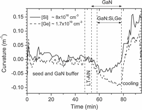
Figure 1: In-situ curvature measurement of Magdeburg’s Si/AlN/2x(GaN/LT-AlN/) GaN/GaN:Si,Ge layer stack.
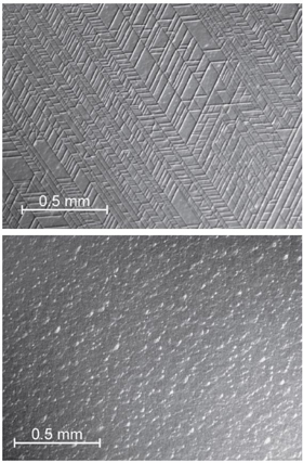
The development of the curvature of the wafer during growth (Figure 1) was determined using an in-situ optical system supplied by LayTec. The curvature indicates the stress development in the nitride semiconductor layers. While the compressive stress induced by the GaN/AlN layers turns tensile during silicon doping, the compressive trend continues with germanium doping. The germanium-doped sample stress only turns tensile during cooling, as expected. Cracks develop in the Si-doped sample, but not in the Ge-doped material (Figure 2).
 Figure 2: Nomarski microscopy images of the Si (top, 8x10¹⁸/cm3) and Ge (bottom, 1.7x10¹⁹/cm3) doped samples.
For the Ge sample, the carrier concentration (1.7x10¹⁹/cm3) was determined using C–V measurements. Due to the cracks, the Si sample electron concentration could not be measured in this way. Instead, identical conditions were used to grow a Si-doped GaN layer on sapphire, which had a C–V carrier concentration of 8x10¹⁸/cm3.
X-ray diffraction analysis revealed the tensile stress of the Si-doped GaN to be 4.4x10⁻³, while that in the Ge-doped sample was 2.7x10⁻³. The full-width at half maximum (FWHM) of the x-ray (0002) diffraction peak was 400arcsec for Ge-doped GaN and 700arcsec for Si doping. The narrower peak for the Ge-doped sample indicates superior crystal quality.
The photoluminescence of the Ge-doped sample was a factor of two more intense than that of the Si-doped material.
The Magdeburg researchers suspect that silicon nitride forms the cores of the dislocations that lead to tensile stress and eventually cracking. The team observes that the germanium analog, Ge3N4, is not stable under MOCVD GaN growth conditions (near the compound’s melting point of 900°C).
Although germanium-doping is applicable to AlGaN layers, the ionization increases with increasing Al content, reducing the material’s doping effectiveness.
The researchers believe that the technique could also be applied to hydride vapor phase epitaxy (HVPE), which is used to create very thick GaN layers.
Germany’s Bundesministerium für Bildung und Forschung (federal education and research ministry) provided some funding for the work within its GaNonSi project.
The author Mike Cooke is a freelance technology journalist who has worked in the semiconductor and advanced technology sectors since 1997.
