- News
21 January 2011
KLA-Tencor launches HB-LED inspection tool for improved substrate and MOCVD process control
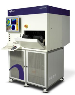
 Process control and yield management solutions provider KLA-Tencor Corp of Milpitas, CA, USA has launched the Candela 8620 substrate and epitaxy wafer inspection system, which is designed to provide automated defect inspection for high-brightness light-emitting diode (HB-LED) materials such as gallium nitride, sapphire and silicon carbide, enabling enhanced quality control of both opaque and transparent substrates, faster time-to-root cause, and improved metal-organic chemical vapor deposition (MOCVD) reactor uptime and yield.
Picture: Candela 8620 substrate and epiwafer inspection system.
With proprietary optical design and detection technology, the Candela 8620 detects and classifies sub-micron defects that are not consistently identified by existing inspection methods, it is claimed, enabling for the first time a production line monitor for these yield-limiting defects. As HB-LED manufacturers transition production to larger wafer sizes and introduce new patterned sapphire substrate (PSS) processes, the economic impact of resulting process-induced defects is estimated to be millions of dollars in lost product revenue per year, and MOCVD epi process issues may result in as much as 40% of overall defect-induced yield loss, KLA-Tencor says.
“The enhanced performance of KLA-Tencor’s Candela 8620 is an important part of our yield and cost-reduction efforts,” comments Iain Black, VP of manufacturing engineering and innovation at LED maker Philips Lumileds of San Jose, CA, USA, an early adopter of the Candela 8620 system. “The system has been an important element in accelerating our process ramp as we transition to 150mm substrates and is allowing us to select sapphire vendors with the highest quality,” he adds.
Defects from substrate and epi processes impact device performance, yield and field reliability. The Candela 8620 can detect:
- Substrate defects such as micro-scratches and micro-cracks, which can create epi process defects and directly impact LED yield and reliability;
- Defect sources from lithography and etch processes for patterned sapphire such as missing bumps and resist voids, resulting in epi defects or reduced lumen output;
- Macro- and micro- defects in MOCVD processes, including hexagonal pits and bumps leading to electrical failure, and epi cracks, which can adversely impact field reliability.
LED substrates and epilayers pose significant inspection challenges due to high levels of background signal and nuisance defects, says KLA-Tencor. The Candela 8620’s imaging and detection system is optimized to enhance the signal from relevant defects-of-interest while suppressing background noise. Aided by its multi-channel detection optics, the system also allows high-purity classification of such defects, allowing comprehensive statistical process control of critical MOCVD processes.
“KLA-Tencor is leveraging more than three decades of expertise in semiconductor process control to benefit customers in emerging markets like HB-LED,” says Jeff Donnelly, group VP of Growth and Emerging Markets. “Recently, several HB-LED manufacturers have installed the Candela 8620 system, and the system's proven ability to identify hard-to-detect defects allows customers to realize higher substrate quality and maximize return on MOCVD investment,” he claims.
KLA-Tencor currently has hundreds of Candela tools installed around the world. Candela is part of KLA-Tencor’s integrated HB-LED portfolio, which includes the ICOS WI-2220 and WI-2250, and Klarity LED. Candela tools are backed by KLA-Tencor’s global, comprehensive service network.
KLA-Tencor HB-LED inspection tool HB-LEDs MOCVD
