- News
16 August 2011
Blocking and reflecting to increase nitride LED light output
National Cheng-Kung University and Kun-Shan University in Taiwan have used silicon dioxide/aluminum structures under the p-electrodes of nitride semiconductor LEDs to improve light output [Chun-Fu Tsai et al, Semicond. Sci. Technol., vol26, p095013, 2011]. The silicon dioxide (SiO2) was used to spread the current from the p-electrode over a wider area of the active region structure and the aluminum (Al) created a reflector to reflect light that would be absorbed by the p-electrode for extraction instead from the sapphire side.
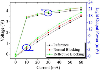
 Figure 1: Light output power/current versus voltage (L–I–V) curves of the reference, normal blocking and reflective blocking LEDs.
Three devices were produced: one with no structure (reference); one with a SiO2 current blocking/spreading structure (normal blocking); and a final one with a SiO2/aluminum structure (reflective blocking). At 20mA injection current, the light output powers were 6.44mW, 7.45mW and 8.1mW, for the reference, normal blocking and reflective blocking devices, respectively. These represent improvements over the reference of 15.7% for the normal blocking LED and 25.8% for the reflective blocking device. Beyond 20mA, the blocking devices continue to show improved performance over the reference (Figure 1).
Nitride LEDs grown on insulating sapphire substrates usually have their p- and n-electrodes on the nitride side of the device. The electrodes tend to interfere with the ability to extract light from the structure. However, by reducing the electrodes to enhance extraction, one also increases the current density flowing through certain regions of the LED (e.g. under the p-electrode). Unfortunately, high current densities are a particular problem in nitride LEDs, where the efficiency can ‘droop’ drastically at high current. Also light produced directly beneath the p-electrode will more likely be absorbed by it.
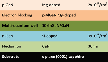
 Figure 2: Schematic cross-section of nitride semiconductor epitaxial structure used for LEDs.
The nitride semiconductor epitaxial structures (Figure 2) were grown on c-face (0001) sapphire using metal-organic chemical vapor deposition (MOCVD) in a rotating-disk reactor with trimethyl-metal and ammonia sources. The silicon/n- and magnesium/p-type doping came from silane and biscyclopentadienyl-magnesium, respectively. The mesa structure of the LED was patterned using photolithography and cut using inductively coupled plasma etch, before producing the different blocking designs for experimental tests.
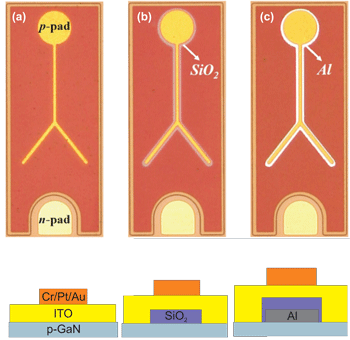
 Figure 3: (top) CCD images of (a) reference, (b) normal blocking and (c) reflective blocking LEDs and (bottom) corresponding cross-sectional schematic views of the CBL structures.
The ‘normal’ blocking sample (Figure 3) consisted of silicon dioxide, deposited using plasma-enhanced CVD and patterned and wet etched with photolithography and a buffered oxide etch solution. The new ‘reflective’ blocking sample added aluminum with a reflectivity of 91% in 430–480nm blue light range. A ‘reference’ sample without blocking structure was also produced.
The 250μm x 580μm LEDs were completed with 250nm transparent conducting layers of indium tin oxide (ITO) on top of the current-blocking structures and chromium/platinum/gold metal p-/n-contact pads. The LEDs were all produced from epitaxial material grown on one substrate to ensure that improvements were caused by the current-blocking and reflection structures.
The electroluminescence peaks of the three devices occurred around 454–455nm with full-width half-maxima (FWHM) of 18nm. The heights of the peaks went in lowest-to-highest order: reference, normal blocking, and finally reflective blocking.
Beam-profile/near-field images showed that the effect of the current-blocking structures was to spread out the current injection, reducing the current density in the active region to a level where photon production is more efficient.
The reverse-bias characteristics of the devices were also improved with the current-blocking structure. The reverse currents at 5V were 33.2nA, 20.7nA and 29.3nA, respectively, for the reference, normal blocking and reflective blocking devices. The researchers suggest that the improvement was due to the passivating effect on surface defects of the silicon dioxide blocking layer. There is less silicon dioxide in contact with the p-GaN contact in the reflective blocking case.
The forward voltages of the blocking devices (both, 3.7V) at 20mA were slightly higher than for the reference (3.6V). This is attributed to larger series resistance due to the smaller contact area between the p-GaN and transparent conducting indium tin oxide electrode. The reference also has a shorter average conduction path, since less spreading occurs.
The author Mike Cooke is a freelance technology journalist who has worked in the semiconductor and advanced technology sectors since 1997.
