- News
24 November 2010
SiN raises nitride HEMT breakdown without current collapse
The University of Sheffield and the UK defense research company QinetiQ have developed techniques for using silicon nitride passivation to increase breakdown voltages without current collapse in nitride semiconductor high-electron-mobility transistors (HEMTs) [K B Lee et al, Semicond. Sci. Technol., vol25, p125010, 2010].
HEMTs using gallium nitride (GaN) with an aluminum gallium nitride (AlGaN) barrier layer grown on silicon carbide substrates have achieved a record 41W/mm power density at 4GHz. However, at high frequencies the current that can pass through such devices collapses, impacting device performance. These devices have also been developed for high-power operation, where a high breakdown voltage is desired.
Different types of silicon nitride (SixNy) films have been used both to mitigate ‘current collapse’ and to increase breakdown voltages. However, the effects of the different films work against each other. The Sheffield–Qinetiq research was directed at finding ways to combine the different films to produce high breakdown voltages without current collapse.
The Sheffield–Qinetiq HEMT device structures consisted of Al0.22Ga0.78N/GaN/sapphire substrate (2-inch diameter), grown using metal-organic chemical vapor deposition (MOCVD). The carrier density of the two-dimensional electron gas (2DEG) that forms at the AlGaN/GaN interface was 6.5x1012cm2, with a mobility 1200cm2/V-s.
This material was used to create HEMTs with 0.25μm gate length and 0.48μm gate–drain separation. Some test structures were also made to allow the researchers to separate out the impacts of surface and bulk leakage currents on performance.
The HEMT mesas were formed using inductively coupled plasma etching. The ohmic source/drain contacts consisted of titanium-aluminum-titanium-gold layers. The Schottky gate metal structure was nickel-gold.
The silicon nitride bilayer passivation consisted of stoichiometric Si3N4 (std-SiN) followed by low-temperature SixNy (LT-SiN). The passivation was deposited in a plasma-enhanced chemical vapor deposition (PECVD) system at 300°C and 30°C, respectively. Various thicknesses for these layers were investigated (including zero).
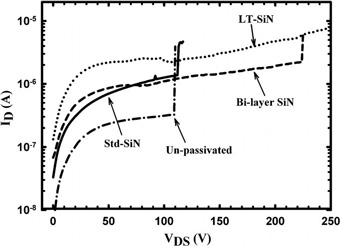
 The three-terminal breakdown measurements were carried out on at least 50 devices. In one test for breakdown (Figure 1), devices with 200nm SiN passivation were compared with unpassivated devices at a gate voltage (Vgs) of –7V. Three types of passivation were compared: std-SiN, LT-SiN, and a bilayer with std-SiN:LT-SiN of 1:3. Both the unpassivated and std-SiN devices showed breakdown occurring around 120V source–drain voltage (Vds).
Figure 1: Three-terminal breakdown measurements for HEMT devices passivated with various SixNy films at pinch off (Vgs = –7 V). Thickness ratio for std-SiN-LT-SiN bilayer passivated device is 1:3. Total thickness of passivation film is 200nm.
The breakdown performance was more than doubled to 250V by using LT-SiN passivation. The bilayer device also showed improved breakdown performance, sustaining up to around 225V.
Such improvement using LT-SiN has been seen before and has been attributed to the suppression of conduction and the ionization of surface states on the AlGaN barrier layer. However, the Sheffield/Qinetiq researchers are skeptical of this interpretation on the basis of surface-leakage and capacitance–voltage (CV) measurements on their test structures: “We propose that the increase of the breakdown voltage in the LT-SiN passivated structure is caused by the moderation of the electric field at the drain edge of the gate”. The moderation is likened to that achieved using field-plate structures.
In fact, the surface leakage current increases by about one order of magnitude after LT-SiN passivation. By contrast, std-SiN reduces surface leakage by about two orders of magnitude. The CV measurements carried out at 10kHz and 1MHz indicate that the LT-SiN passivation has a higher surface trap density compared with std-SiN.
The Sheffield/Qinetiq research suggests that the electric field moderation comes about through tunneling of carriers from the gate into the LT-SiN trap states at pinch-off. These trapped charges reduce the peak field, increasing the breakdown voltage.
Current collapse was gauged using pulsed measurements with devices being kept below pinch-off and then the gate voltage is pulsed for 400ns to full channel current. The headline figure in these measurements is the ‘gate lag response’ (GLR), the fraction of the pulsed current of the normal DC value. In unpassivated devices, the GLR was 50%. With 200nm passivations, the GLR was near 100% for std-SiN but less than 40% for LT-SiN. The GLR was maintained at near 100% for bilayers with std-SiN:LT-SiN ratios of 1:3 and 1:1.
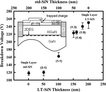
 Various bilayer combinations were tested for breakdown (Figure 2). Clearly decreasing the std-SiN thickness is advantageous for high breakdown voltage. With 20nm of std-SiN, the breakdown is at 238V. With std-SiN layer of more than 150nm, the breakdown settled to a value of ~120V — that of the single std-SiN layer device. The thickness of the LT-SiN is found to be less critical — devices with std-SiN layers of 50nm but different LT-SiN layers of 150nm and 350nm had breakdowns at about 225V. This suggests that the charge trapping that gives a field-plate-like effect occurs predominantly at and/or near the interface between the two materials.
Figure 2: Std-SiN:LT-SiN thickness ratios dependent breakdown voltage, VB, of the bi-layer SixNy passivated HEMTs at pinch off, Vgs = –7V. The total thickness of the SixNy film is 200 nm. Inset: bi-layer passivated devices with charge trapped at the interface between LT-SiN and std-SiN.
The point seems to be that the thinner the std-SiN, the nearer the trapped charge is to the semiconductor, allowing the charges to more effectively modify the electric field and thus increase the breakdown voltage.
The Sheffield/Qinetiq work was funded by the Electro-Magnetic Remote Sensing (EMRS) Defence Technology Centre, established by the UK Ministry of Defence and managed by a consortium of companies — Selex, Thales Defence, Roke Manor Research and Filtronic.
The author Mike Cooke is a freelance technology journalist who has worked in the semiconductor and advanced technology sectors since 1997.
