| Home | About Us | Contribute | Bookstore | Advertising | Subscribe for Free NOW! |
| News Archive | Features | Events | Recruitment | Directory |
News
24 June 2010
IMEC’s CMORE service extended with SiGe-MEMS foundry and MPW runs
International microelectronics research center IMEC of Leuven, Belgium has extended its CMORE service with SiGe-MEMS foundry and (for universities and research centers) multi-project wafer (MPW) runs (via IMEC’s EUROPRACTICE IC scheme). Both the SiGe-MEMS foundry and MPW services are both on IMEC’s monolithically integrated SiGe MEMS (micro-electromechanical system) baseline process and come with an extended design kit.

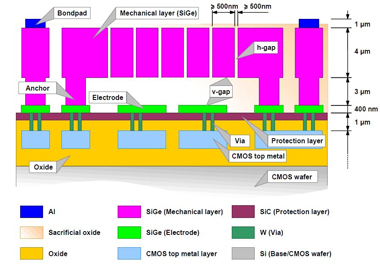
Image: Cross section of device created with IMEC's baseline SiGe-MEMS platform.
Via its CMORE initiative, IMEC offers companies the services needed to turn concepts into packaged microsystem products. The CMORE toolbox contains a wide variety of device technologies (e.g. high-voltage technologies, CMOS imagers, photonics or MEMS) and packaging capabilities (e.g. through-silicon vias and MEMS capping) as well as design expertise and testing and reliability know-how.
IMEC’s services range from feasibility studies over design and technology development to prototyping and low-volume manufacturing. Also, through its alliance with Taiwan’s TSMC (the world's biggest silicon wafer foundry), IMEC can also offer a path to transfer the technology to the foundry for volume production.
The SiGe-MEMS platform’s technology is based on a MEMS-last approach, where the MEMS are processed after and on top of the CMOS circuits. This enables monolithic integration of CMOS and MEMS, integrating MEMS devices with the driving and readout electronics on the same die. IMEC claims that this leads to better performance compared with other integration schemes: there is a better signal-to-noise ratio through reduced interconnect parasitic resistance and capacitance, a smaller die size and package, and lower power consumption.
The CMORE SiGe-MEMS platform is a flexible and modular approach that allows application-specific tuning and optimization. An example is the thickness of the MEMS structural layer, which can vary between 300nm and 4µm. A 300nm-thick layer allows the fabrication of optical MEMS (e.g. micro-mirrors). The process is then extended to add various coatings with specific reflective properties. A 4µm structural layer is used, for example, to create gyroscopes or actuators. Other possible applications of the technology are µ-microphones, µ-speakers, µ-sensors, µ-mirrors, probe-based memories and µ-power generation.
The extended CMORE offering and foundry service is based on the SiGe-MEMS platform, fixing the options in a baseline process with a 4µm SiGe mechanical layer on top of a CMOS layer. Supported by mature design kits for the most important commercial MEMS design tools, partners can develop their own MEMS designs for rapid prototyping.
For universities and research centres, by gathering the designs of multiple customers on the same mask set, the MPW service allows the fabrication of test structures and prototypes of devices at low cost. A first MPW run, scheduled for the end of 2010, will be processed on a wafer with a single metal layer, and is intended for initial prototyping. A second run, with full capability and with the SiGe-MEMS devices on top of TSMC’s 0.18µm CMOS, is scheduled for mid 2011.
![]() Search: IMEC SiGe-MEMS foundry
Search: IMEC SiGe-MEMS foundry
Visit: www.imec.be/cmore