| Home | About Us | Contribute | Bookstore | Advertising | Subscribe for Free NOW! |
| News Archive | Features | Events | Recruitment | Directory |
News
23 February 2010
Agilent launches first single-box analyzer/curve tracer for 40A/3000V power devices
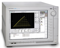
 Agilent Technologies Inc of Santa Clara, CA, USA has introduced enhancements to its B1505A Power Device Analyzer/Curve Tracer to make it what is claimed to be the first single-box solution able to characterize semiconductor devices up to 3000V and 40A (compared to 20A when originally launched in November 2008), available for ordering from 1 May.
The high-power device market is growing rapidly each year due to the demand for green engineering and products that conserve energy, says Agilent. Industry segments leading the growth are hybrid and other high-efficiency cars; industrial uses such as robotics, solar cells, wind electricity and electric trains; and, in information technology and consumer electronics, CPU power control circuits that require a highly efficient power device for power conservation.
Silicon-based power MOSFET and IGBT (insulated-gate bipolar transistor) devices are being engineered to reduce energy loss, conserve power and decrease operating costs. However, some new devices are using wide-band gap materials such as silicon carbide (SiC) or gallium nitride (GaN) to achieve high efficiency. In addition, on-wafer testing has become very important for reducing development turnaround times. The upgrade to 40A capability increases the number of power devices and applications that the B1505A can serve, says Agilent.
"Test and measurement of high-power devices is a growing requirement for manufacturers, yet one that demands the utmost accuracy and reliability," says Masaki Yamamoto, general manager of Agilent Hachioji Semiconductor Test Division. "Researchers and development engineers need to know they can be confident in their findings," he adds. "On-wafer as well as packaged device 40A evaluations are strong requirements in the marketplace because they help dramatically decrease time to market.”
The B1505A is a single-box solution that provides for ease of use and ease of analysis. Its new 40A capability comes from its ability to support two high-current source monitor units (HCSMUs) in a single device. Existing B1505A owners with a HCSMU can easily add a second HCSMU with an accessory to enable 40A sourcing and measurement for both packaged and on-wafer devices. Agilent says that the all-in-one design provides a simple and clean configuration for 40A sourcing and measurement, allowing easy set-up and providing an uncluttered work environment with space for larger devices. Also, the new design is unlike a measurement system built with multiple instruments, where complicated cabling and user safety considerations are required.
The B1505A can measure currents up to 40A and display the results in various formats, including semi-log or log-log graphs with extracted parameters. The interlock feature ensures safe operation by preventing electrical shock even with the increased current capacity. The module selector supports automatic switching between multiple types of SMU; this allows the measurement of key parameters, such as on-resistance and breakdown voltage in a single measurement sequence. The tracer test mode, which now covers 40A as well as newly developed simultaneous sweep range control in positive and negative directions, provides intuitive and easy-to-use measurement with the same look and feel of the existing B1505A.
Also provided is a new socket module to support the test adapters widely used by conventional curve tracer users, allowing reduced migration costs when replacing old curve tracers with the B1505A.
Key features of the B1505A include:
- device characterization at 3000V and 40A in a single instrument with accuracy down to sub-pA;
- new accessories that allow clean and safe connection for 40A measurement for packaged devices and on-wafer devices;
- capacitance-voltage (CV) measurements with high DC bias up to 3000V;
- a new accessory that supports test adapters widely used in conventional curve tracer; and
- simultaneous sweep range control in positive and negative directions.
![]() Search: Agilent SiC GaN Test and measurement
Search: Agilent SiC GaN Test and measurement
Visit: www.agilent.com/find/B1505A