- News
28 December 2010
Substrate removal and reflector layer boost red LED output
Researchers based at National Cheng Kung University and WuFeng University in Taiwan have developed techniques to boost the output from red light emitting diodes constructed using aluminum gallium indium phosphide (AlGaInP) semiconductor structures. [Der-Ming Kuo et al, Appl. Phys. Express, vol4, p012101, 2011].
Although AlGaInP LEDs can achieve 90% internal quantum efficiency, high extraction efficiencies are hampered by absorption in the gallium arsenide (GaAs) substrate used to grow these devices.
The researchers did use GaAs substrates to grow the epitaxial structure using metal-organic chemical vapor deposition. However the substrate was later removed using a wet etch employing ammonium hydroxide/hydrogen peroxide solution (NH4OH:H2O2:H2O, 1:4:2 for two hours). The epitaxial structure consisted of n-GaAs buffer (300nm), InGaP (200nm), n+-GaAs (50nm), n-AlGaInP (2μm), n-AlInP cladding (50nm), AlGaInP/InGaP multi-quantum well active layer, p-AlInP cladding (50nm), and p-GaP contact (9μm).
On top of these layers plasma-enhanced chemical vapor deposition was used to create a silicon dioxide diffusion barrier (0.5μm thick) that was then patterned into 280x280μm squares. The metal part of the p-contact consisted of gold-beryllium alloy (150nm) and gold (350nm) covering a 300x300μm area. Then a 450°C anneal was used to achieve ohmic behavior with high reflectivity (85%).
 The purpose of the silicon dioxide barrier was to restrict the region of contact between the metal and the p-GaP. To make an ohmic contact the metal has to be thermally annealed and this causes some metal to diffuse into the p-GaP, roughening the interface and reducing reflectivity.
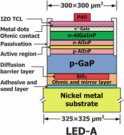
To prepare for nickel electroplating, an adhesive/seed layer consisting of chromium, titanium and gold (100nm each) was deposited using electron-beam evaporation. The nickel substrate was grown to a thickness of 80μm to serve as substrate for the final device (Figure 1a).
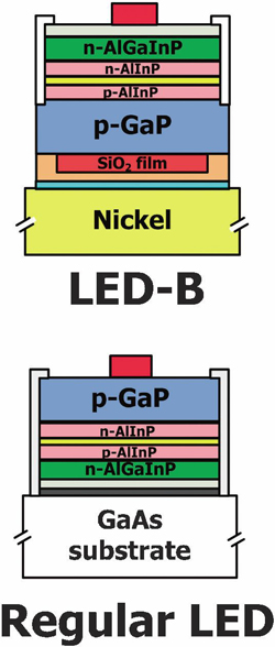
Figure 1: Schematic of (a) LED-A, which has a Ni substrate and IZO TCL. (b) LED-B, which has a Ni substrate but without IZO TCL (top), and a regular LED with a GaAs absorbing substrate (bottom). All devices have same chip size of 300x300μm.
 It was at this point that the GaAs substrate was removed, along with the InGaP layer (using hydrochloric/phosphoric acid solution), exposing the thin n+-GaAs layer.
The n-contact consisted of 10μm-diameter ohmic-contact metal dots of germanium-gold alloy (95nm) and gold (200nm). After the metal dots were annealed at 360°C, 300nm of indium zinc oxide (IZO) was applied using sputtering, to create a transparent conducting layer with transmittance above 87%. The researchers found that IZO on its own formed a Schottky contact with n+-GaAs, but that adding the metal dots created an ohmic contact for the system. Presumably the dots provide a low resistance conduction path between the n+-GaAs/IZO materials.
The 300x300μm device mesas separated by 25μm were then wet etched down to the p-GaP layer using hydrochloric/phosphoric acid solution. A metal pad for the p-contact and passivation were finally deposited.
Two other LEDs were created for comparison purposes (Figure 1b): an LED using a similar process to that already describe, but without the transparent conducting layer; and, an LED produced conventionally with GaAs substrate. The peak emission wavelength was around 624nm (red) for all three devices.
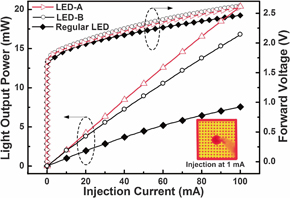
Voltage and light output power dependence on current was determined (Figure 2). The nickel/IZO contact devices had a 0.02V increase in forward voltage at 20mA compared with the regular LED. This is attributed to the presence of the resistive silicon dioxide diffusion barrier needed to improve the reflectivity of the p-contact. The IZO contact improved the forward voltage at 20mA by about 0.03V, compared with the device without such a contact (LED-B). This improvement is attributed to the IZO reducing current crowding effects, hence reducing the resistance of the contact.
 Figure 2: Comparisons of current-voltage and light output power-current characteristics between LED-A, and comparison devices (LED-B, and regular LED). Inset shows photo of light emission from LED-A at injection current of 1mA.
Despite the reduced electrical performance, the nickel/IZO devices (LED-A) increase light output power (4.225mW) significantly by 116.7% at 20mA and 168.9% at 100mA over the regular device (1.95mW). Even without the IZO layer, LED-B (3.75mW) showed a 92.5% in light output at 20mA over the regular device.
The further improvement in using an IZO film is attributed to reduction in total internal reflection at due to its refractive index (2.1) being closer to that of air (1), compared with GaAs (3.8). The lower refractive index increases the critical angle that determines which photons can leave the structure.
The researchers note that their devices do not reach the external quantum efficiency (EQE) of commercial devices. The full device achieved an EQE of 10.5% at 20mA. The comparison device without IZO had an EQE of 9.3% at 20mA, and the regular device 4.9%. These low values are attributed to the low material quality of the epitaxial wafers, compared with those available commercially (EQE up to ~50%).
‘Nevertheless, results obtained from the comparisons of current-voltage and light output power characteristics of the prepared samples still clearly reveal the effectiveness of the proposed technology for AlGaInP LEDs,’ the researchers maintain.
The author Mike Cooke is a freelance technology journalist who has worked in the semiconductor and advanced technology sectors since 1997.
