| Home | About Us | Contribute | Bookstore | Advertising | Subscribe for Free NOW! |
| News Archive | Features | Events | Recruitment | Directory |
News
9 April 2010
Tunneling a way to understand efficiency droop in InGaN LEDs
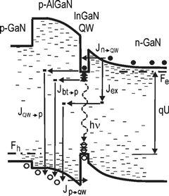
Researchers based in St. Petersburg, Russia, have turned their attention to the droop in light-emission efficiency with electrical current in nitride semiconductor light-emitting diodes [N.I. Bochkareva et al, Appl. Phys. Lett., vol96, p133502, 2010]. The collaboration suggests a droop mechanism involving tunneling leakage of carriers from the quantum well (QW) to defect states in barriers, and a reduction in carrier injection efficiency through an excess tunneling current between deep defect states in the barriers, bypassing the QW (Figure 1). The work involved A.F. Ioffe Physical-Technical Institute, St.-Petersburg State Polytechnical University and V.F. Fock Institute of Physics.
 Figure 1: St. Petersburg defect-related tunneling model for a p-n structure with an AlGaN/InGaN/GaN QW. As the potential difference between the injection regions pushes the quasi-Fermi levels to the band edges, new current paths become available from the QW to deep defects in the p-type barrier (JQW->p). Also, localized states that create lower-frequency emissions are killed by a similar mechanism at lower forward voltages
(Jbt->p). The hole and electron injection currents into the well are Jp->QW and Jn->QW, respectively. The excess current operates through tunneling between defect states in the two barrier regions (Jex).
As evidence for these tunneling-related mechanisms, the scientists cite three experimental results of their work: the efficiency droop occurs in the low-energy part of the photon emission spectrum; the forward voltage where the efficiency droop sets in (~2.9V) is independent of temperature (77–300K); and, at forward voltages greater than the maximum efficiency voltage, the diode ideality factor is greater than 2 (4.4 at 300K).
An ideality factor greater than 2 can be a signal for Auger recombination, which is one of the more popular explanations for efficiency droop effects in nitride LEDs. ‘Auger recombination’ refers to a mechanism where the energy from a recombination event is given to another carrier, rather than being emitted as light, reducing the light-emission efficiency. Since Auger recombination involves three carriers, it is only expected to occur at higher currents.
In opposition to such an explanation, the St. Petersburg researchers point to a reduction in the efficiency peak current at lower temperatures (0.47mA at 300K, 7μA at 90K) and comment: “This efficiency decrease at low currents can hardly be attributed to Auger recombination.”
The constancy of the forward voltage where maximum efficiency occurs is also seen as significant, since it gives electron energies close to the bandgap of the well material (2.89eV). The researchers suggest that this maximum efficiency forward voltage is when the quasi-Fermi levels in the barriers reach the relevant band edge in the well (bottom of conduction band; top of valence band — see Figure 1).
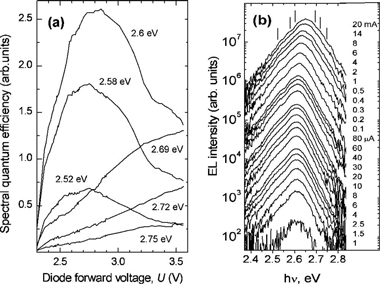
These effects would particularly hit localized carrier states that are often cited as the reason for the surprisingly high efficiencies of nitride semiconductor LEDs. Recombination from these states is a slow process, and faster non-radiative channels would have a larger effect in killing their efficiency. The reduction in efficiency in these longer-wavelength states leads to a blue-shift in the emission spectrum (Figure 2).

Figure 2: (a) Spectral efficiency of electroluminescence (EL) vs diode forward voltage for different spectral regions. (b) Room-temperature EL spectra at various driving currents.
The LEDs used in the work (from Nichia, model NSPB-500S) were grown on sapphire substrates with an active region consisting of a single 30Å indium gallium nitride (In0.2Ga0.8N) QW. The n-type injection region was 4μm of GaN. A p-type barrier consisted of 100nm of aluminum gallium nitride (Al0.2Ga0.8N). The emission wavelength was about 470nm (blue).
The epoxy-encapsulated LEDs were mounted on a cold finger of a cryostat chamber for temperature control. The LEDs were tested under continuous-wave (DC) operation. Room-temperature studies often use pulsed operation to avoid self-heating of the devices from resistance effects. This is not necessary for deliberately cooled devices.
See related items:
Auger largely responsible for limited LED efficiency
InGaN LED spillover and efficiency droop
Following the thread of LED efficiency droop
RPI cuts LED efficiency droop via polarization-matched GaInN/GaInN MQWs
Fathoming efficiency droop in InGaN MQW-LEDs
See article: Solutions don’t solve droop controversy
![]() Search: InGaN LEDs Droop
Search: InGaN LEDs Droop
Visit: http://link.aip.org
The author Mike Cooke is a freelance technology journalist who has worked in the semiconductor and advanced technology sectors since 1997.