| Home | About Us | Contribute | Bookstore | Advertising | Subscribe for Free NOW! |
| News Archive | Features | Events | Recruitment | Directory |
| FREE subscription |
| Subscribe for free to receive each issue of Semiconductor Today magazine and weekly news brief. |
News
8 October 2009
Optoexcitonics comes in from the super-cold
Fast, compact optoelectronics is the aim of “proof-of-principle” devices being developed at the University of California at its San Diego (UCSD) and Santa Barbara (UCSB) sites [Grosso et al, Nature Photonics, vol.3, p.577, 2009]. Researchers have boosted the operating temperature for demonstrations of exciton optoelectronic devices from ~1.5K (~–270°C) to ~100K (~–170°C). This brings the potential for the technology out of the arena of small-scale laboratory cryogenic conditions into the more commercial cooling supplied by standard liquid nitrogen sources. Ultimately, however, UCSD wants to create room-temperature devices.
Excitons roughly speaking consist of bound states of electrons from the conduction band and holes in the valence band. The excitonic devices explored at UCSD are based on controlling the flow of excitons using electrodes and having either excitons or photons as input/output. The performance depends on the transformation of photons into excitons and vice versa.
The UCSD team sees two advantages for excitonic processing of the photonic signals – high interconnection speed and compactness/scalability.
High speed results from the direct photon-exciton coupling rather than through the rather optically inactive medium of electrons. Normally, the need to convert photonic signals to electrons and then possibly back into photons introduces delays, slowing down operations. This delay would be eliminated in exciton-based signal processing.
Compactness is achieved through the use of micron-scale semiconductor technology rather than the 100μm of even the smallest Mach-Zehnder modulator or similar photonic device. This is achievable because the de Broglie wavelength of the exciton is much shorter than that of the light to which it couples.
Limits on the use of excitons concern the lifetime and binding energy of the quasi-particles. Normal “direct” excitons have lifetimes before recombination and emission of photons of less than a nanosecond, restricting the distance the quasi-particles can travel. Further, the binding energy restricts the temperature of operation since shallow binding causes the exciton to split into free electrons and holes under thermal fluctuations.
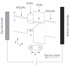
To overcome the short lifetimes, the researchers have developed “indirect” excitons consisting of bound electrons and holes from separated layers (Figure 1). This increases lifetimes by orders of magnitude, depending on the electron-hole layer separation distance, by reducing the overlap of the electron-hole wavefunctions. The excition binding energy depends on the materials and electron-hole separation – the 1.5K devices were based on a GaAs/Al0.33Ga0.67As coupled quantum well structure (CQW) with a 12nm separation giving a binding energy of 40K (energy/Boltzmann’s constant kB). The new ~100K devices use AlAs/GaAs structures and 12nm separation, resulting in an exciton binding of about 100K.
 Figure 1: Schematic band diagram for AlAs/GaAs coupled quantum well structure giving rise to indirect exciton states.
The indirect electron-hole exciton has a dipole moment that can be used to manipulate their movement with the electric field between suitably biased electrodes.
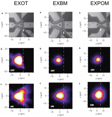
The technology (Figure 2) was used to produce exciton optoelectronic transistors (EXOTs), excitonic bridge modulators (EXBMs), and excitonic pinch-off modulators (EXPOMs). The laser light used to create the excitons is focused on the source electrode in the position of the circles in Figure 2. The photon source was a HeNe laser emitting red light at 633nm wavelength. The operation temperature was 85K, although exciton flow characterization experiments were also carried out up to 200K.

Figure 2: Electrode arrangements and false color images for operation of EXOT, EXBM and EXPOM proof-of-principle devices. The EXOT and EXBM use source, drain and gate electrodes. The EXPOM uses lateral electrodes (a) to control excitonic fluxes in a channel constriction under the c-electrode. In all cases the laser light is directed onto the position indicated by the circle.
The EXOT is a three terminal device that controls exciton flow between two electrodes using a third electrode to provide switching by creating or removing a barrier to exciton flow. The EXBM instead uses a negative gate potential to make the excitons unstable in the gate region. Removing this potential enables to the excitons to cross from the source to the drain. Finally, the EXPOM uses a different electrode arrangement to control the electron flux under a 2μm constriction in the electrode.
The corresponding author on the paper, Alex High, comments: “Although it may not be apparent from the images the contrast between on/off in the output region is large enough (more than three-fold) that a thresholding device could distinguish between the off and on state. Of course, with further optimization of the quantum well structure we hope not only to continue raising the operation temperature but also to improve the quality of operation. For instance, at 125K only a small portion of the excitons travel out of the source electrode, and this could be improved by designing a quantum well structure with a higher binding energy.”
![]() Search: Exciton optoelectronic devices AlAs/GaAs
Search: Exciton optoelectronic devices AlAs/GaAs
Visit: www.nature.com
Visit: http://physics.ucsd.edu/~lvbutov/exot.php
The author Mike Cooke is a freelance technology journalist who has worked in the semiconductor and advanced technology sectors since 1997.