| Home | About Us | Contribute | Bookstore | Advertising | Subscribe for Free NOW! |
| News Archive | Features | Events | Recruitment | Directory |
| FREE subscription |
| Subscribe for free to receive each issue of Semiconductor Today magazine and weekly news brief. |
News
6 November 2009
Sharp hits 35.8% efficiency for triple-junction solar cell
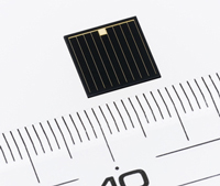
Japan’s Sharp Corp is claiming an efficiency record with its report of a triple-junction compound semiconductor device that boasts a 35.8% efficiency in tests performed in September by Japan’s National Institute of Advanced Industrial Science and Technology (AIST) on a 1cm2 cell (Figure 1).
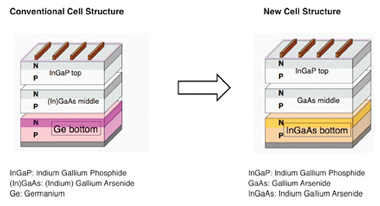
 The device structure consists of an indium gallium arsenide (InGaAs) bottom layer, a GaAs middle layer and an indium gallium phosphide (InGaP) top layer (Figure 2). This differs from the usual range of triple-junction devices, mainly in having InGaAs rather than germanium for the bottom layer.
Figure 1: Sharp’s triple-junction solar cell.
Although germanium is easier to manufacture and can generate a large amount of current, much of the power is wasted. InGaAs has high light-utilization efficiency, but is much more difficult to produce with the high level of crystallinity that is needed.

Figure 2. Schematic of Sharp’s device structure (right) compared with traditional set-up (left).
Sharp says that it has developed a ‘proprietary’ technology to produce much better InGaAs layers, increasing the resulting triple junction cell from the company’s previous effort of 31.5% to 35.8% in the latest announcement.
This record for monolithic, unconcentrated cells should be distinguished from other recent record announcements for triple-junction cells using concentrator systems. The latter class includes Boeing’s Spectrolab Inc with 41.6% (August 2009), Fraunhofer-Institut für Solare Energiesysteme (ISE) with 41.1% (January 2009), and the US Department of Energy’s National Renewable Energy Laboratory (NREL) with 40.8% (August 2008). The Fraunhofer ISE efficiency was achieved at a light intensity of 454 suns over a 5mm2 area; NREL’s with the equivalent of 326 suns.
The US Defense Advanced Research Projects Agency (DARPA) project, led by the University of Delaware, also claimed a record with 42.8% (July 2007). The DARPA efficiency has not been accepted by NREL, which claims that it is one of only three labs in the world that can validate cell efficiencies. The other labs are based in Germany and Japan. In fact, these other labs are Fraunhofer ISE and AIST.
The DARPA device was tested with “sunlight at standard terrestrial conditions” but, on reading the small print, one finds that it is also a concentrating system and, further, it is non-monolithic, splitting the solar light into three different energy bins (high, medium and low) and directing them onto cells of various light-sensitive materials to cover the solar spectrum. A more recent announcement (September 2009) says: “DARPA recently began the second two-year phase of a four-year program with the VHESC Consortium to raise the system power efficiency of a new class of solar modules to 40% and deliver manufacturable engineering prototype modules.”
See related items:
DARPA awards Energy Focus $3.1m to develop spectrum-splitting solar module
Fraunhofer ISE raises multi-junction solar cell efficiency record to 41.1%
NREL sets solar cell efficiency record of 40.8%
![]() Search: Triple-junction solar cell InGaAs
Search: Triple-junction solar cell InGaAs
Visit: http://sharp-world.com
The author Mike Cooke is a freelance technology journalist who has worked in the semiconductor and advanced technology sectors since 1997.