| Home | About Us | Contribute | Bookstore | Advertising | Subscribe for Free NOW! |
| News Archive | Features | Events | Recruitment | Directory |
News
31 December 2009
AlGaN-cladding-free semipolar laser nears green
Researchers from University of California Santa Barbara (UCSB) and Japan’s Mitsubishi Chemical have been extending the wavelength of AlGaN-cladding-free laser diodes grown on semipolar (20-21) GaN substrates [Anurag Tyagi et al, Appl. Phys. Express, vol3, p011002, 2010]. The pulsed (1kHz repetition, 0.01% duty cycle) wavelength of 506.4nm is the longest reported so far for such devices. Although AlInGaN-cladded semipolar GaN laser diodes have achieved green laser light, the growth of AlInGaN is problematic and UCSB is exploring better ways to achieve the optical confinement delivered by the AlInGaN cladding with a view to the needs of production.
Green laser diodes have been the aim of much development in the past couple of years. The leading desire is to replace the complicated arrangement in the color projector equipment that presently uses second harmonic generation (SHG) to convert non-green laser light into green. A direct green laser diode would enable such equipment to be produced with increased energy efficiency, compactness and reliability, hopefully at reduced cost. Other opportunities could arise from replacement of the bulky solid-state and gas lasers used in other applications.
Although green laser light (520-570nm) has been obtained from the nitride material system on easier-to-produce polar c-plane GaN (0001) substrates, problems can arise from such laser diodes as a result of the spontaneous and strain-induced (piezoelectric) polarization charges, leading to electric fields of up to ~1MV/cm. These fields lead to separation effects between the positive (electron) and negative (hole) charge carriers that one wants to recombine to produce light, reducing the radiation levels. In addition, a blue-shifting of the laser wavelength occurs with increased current levels – this is not desirable in applications where maintaining color consistency is important, such as for color projectors.
Non-polar m-plane oriented GaN (1-101) would seem a solution to such problems, but laser diodes produced on such materials have been limited to wavelengths smaller than 500nm. From quantum wells (QWs) designed to emit under photoluminescence in the 560nm region, one finds that the material quality suffers from a high level of stacking faults that would make electroluminescence difficult to achieve. In fact, UCSB has previously produced laser diodes on m-plane freestanding GaN from Mitsubishi Chemical [You-Da Lin et al, App. Phys. Express, vol2, p082102, 2009]
More luck has recently attended the semipolar (20-21) orientation, with Japan’s Sumitomo Electric Industries (SEI) managing to develop pulsed and continuous-wave LDs emitting at 520nm [Yoshizumi et al, Appl. Phys. Express vol2, p092101, 2009] and 531nm [Enya et al. Appl. Phys. Express, vol2, p082101, 2009], respectively.
As mentioned above, this achievement used a lattice-matched quaternary AlInGaN cladding to confine the optical mode for lasing. The growth of such quaternary layers is difficult to control, since the ideal conditions (temperature, pressure, growth rate, etc) of each of the components (AlN, GaN, InN) are widely different.
The UCSB/Mitsubishi group has previously avoided this problem with shorter-wavelength (violet, blue) laser diodes by dispensing with the cladding layer. Instead, a larger active volume and/or high-indium-content waveguiding layers can be used to create sufficient optical confinement.
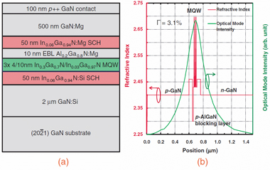
In the latest work, the cladding was provided by GaN rather than AlInGaN (Figure 1). The LD layers were grown using atmospheric-pressure metal-organic chemical vapor deposition on (20-21)-oriented freestanding GaN substrates provided by Mitsubishi Chemical. By using GaN rather than AlGaN, the tendency for cracking is reduced, enabling significantly faster growth rates. The lateral dimensions of the laser diode were 3x1500μm.

Figure 1: Cross-sectional schematic (a) of UCSB laser diode’s layer structure on (20-21) freestanding GaN. The structure includes a 3-period multi-quantum well (MQW), electron blocking layer (EBL), and separate confinement heterostructures (SCHs). This leads to an index profile and calculated optical mode intensity (b) with a transverse confinement factor (Γ) of 3.1%.
The resulting laser diodes had measured threshold current densities of 23kA/cm2 before the application of a high reflective (HR) coating and 19kA/cm2 after. The corresponding threshold voltages were 17.5V and 16V, respectively. These are relatively high values, which the researchers suggest are due to a non-optimized structure and doping profile. The lasing peak in this room temperature (RT) characterization was 504.2nm.
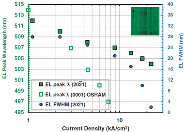
The blue-shift of the device’s spontaneous electroluminescence (EL) with increased current density (Figure 2) was found to be much reduced when compared with published results from Osram for a 515nm c-plane device [Queren et al: Appl. Phys. Lett., vol94, p081119, 2009]. The researchers note that their thresholds were a factor of two larger than that for the longer-wavelength c-plane device. By reducing the threshold, it is hoped that longer-wavelength behavior will be available from UCSB’s (20-21) GaN structure.

Figure 2: Dependence of spontaneous emission electroluminescence (EL) peak wavelength and full-width at half maximum (FWHM) on current density. Peak EL wavelength data for a 500nm c-plane LD developed by Osram are shown for comparison. Inset shows a fluorescence microscope image of the as-grown LD epitaxial wafer.
The characteristic temperature was found from the variation of the threshold current to be about 130K. This compares favorably with the low value of 90K obtained for m-plane LDs. The value also falls within the range of values achieved for c-plane LDs of 120-200K. Higher characteristic temperatures indicate less increase in threshold with an increase in temperature.
The wavelength of the laser radiation also increases (red-shift) with temperature and reaches 506nm at 60°C.
Among the authors of the research paper is Shuji Nakamura, who pioneered much of the development of nitride semiconductors for light and laser emission while at Nichia Corp in Japan during the 1990s. Nakamura joined UCSB as professor in 1999.
See related items:
Sumitomo boosts 520nm green InGaN laser to continuous-wave operation
New angle on approach to green lasers
Sumitomo Electric claims first pure-green semiconductor laser
Osram Opto claims first 500nm InGaN laser
![]() Search: Green laser diodes AlGaN-cladding-free laser diodes GaN substrates
Search: Green laser diodes AlGaN-cladding-free laser diodes GaN substrates
Visit: http://apex.ipap.jp/link?APEX/3/011002
Visit: http://apex.ipap.jp/link?APEX/2/082101
Visit: http://apex.ipap.jp/link?APEX/2/092101
Visit: http://apex.ipap.jp/link?APEX/2/082102
The author Mike Cooke is a freelance technology journalist who has worked in the semiconductor and advanced technology sectors since 1997.

