| Home | About Us | Contribute | Bookstore | Advertising | Subscribe for Free NOW! |
| News Archive | Features | Events | Recruitment | Directory |
| FREE subscription |
| Subscribe for free to receive each issue of Semiconductor Today magazine and weekly news brief. |
News
15 December 2009
Mid-decade timescale for compound/silicon semiconductor integration
“If we can make all of the material integration challenges happen and also make dense devices, then III-V technology could replace silicon technology starting around the middle of the next decade,” says Mike Mayberry of Intel in a ‘guest blog’ on Intel’s latest contributions on III-V transistor on silicon research at the International Electron Devices Meeting (IEDM) last week (7-9 December 2009). Although Mayberry is not in the author list of any of the IEDM papers, he is director of components research at the firm, alongside his role as vice president of technology and manufacturing.
The focus for Intel’s latest reported work has been on the transistor’s gate contact, and particularly reducing leakage through using high-k dielectric insulation, rather than a Schottky contact [Radosavljevic, IEDM session 13.1, December 2009]. A composite gate stack on In0.7Ga0.3As was made using 4nm of tantalum silicon oxide (TaSiOx) and 2nm of indium phosphide (InP). The process steps to produce the stack consisted of cleaning, depositing a thin transition layer and then the dielectric.
A quantum well channel was used in a field-effect transistor (QWFET) format. The work was carried out jointly with researchers from epiwafer foundry IQE based in Bethlehem, PA, USA. The Intel part of the work was based in Oregon. This particular piece of work targets low-power logic applications. However, compound semiconductor properties, such as high frequency or light emission, could also create new highly integrated components and enable technologies such as on-chip optical interconnects.
IQE’s Bethlehem facility produced the semiconductor layer structures as InGaAs QWFET epiwafers grown on silicon substrates using molecular beam epitaxy (MBE). Intel then used the blanket epiwafers for their transistor design and fabrication.
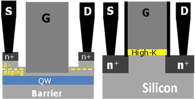
Intel is continuing to work with In0.7Ga0.3As QWFET devices with a Schottky gate contact [Dewey et al, IEDM session 20.2, 2009], comparing logic performance against that of advanced strained Si MOSFETs with supply voltages between 0.5 and 1.0V, at constant Ioff (Figure 1).

Figure 1 (above): Traditional QWFET with Schottky barrier (left) and CMOS transistor with insulated gate to reduce leakage (right).
Modeling work – involving Stanford University, Intel and the US Naval Research Lab – has also been carried out on producing the other component of complementary circuit designs: increased hole mobility [Nainani et al, IEDM session 35.3, 2009]. While hole mobility in silicon is reduced by a factor of three compared with that of electrons, the situation is often much worse in compound semiconductors (typically, a factor of 20-100 lower). The calculations suggest that a strained indium gallium antimonide (InGaSb) combination could achieve better hole mobility. Experiments with In0.41Ga0.59Sb/GaSb resulted in the highest reported hole mobilities, at 3x that achieved with uniaxially strained-Si.
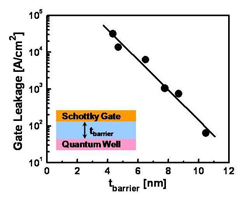
 Figure 2: Gate leakage versus barrier thickness.
Mayberry believes that Intel and its collaborators at other companies and at various universities have made great progress on many of the challenges to integrating III-V transistors with silicon infrastructure. Demonstrated work in meeting these challenges include: building N-channel quantum well devices on a silicon substrate with equivalent performance to those grown on III-V substrates; enhancement-mode (normally-off) device operation; integrating high-k dielectrics on N-channel with good performance; and fast P-channel devices to match N-channel devices for complementary circuit designs.
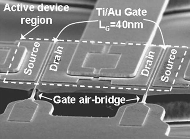
One challenge is a work-in-progress: miniaturization (Figure 3). Presently, although the gate lengths are tens of nanometers, the associated contacts are relatively massive (i.e. micron-scale). To some extent, these are needed to ease the characterization of the transistor structures, but ultimately must be reduced drastically to compete with future silicon transistor formations.

Figure 3 (above): Research InSb p-channel QWFET with 40nm gate length (the thin wire structure between the source and drain electrodes – the gate ‘length’ is in fact of the order of the width of the wire).
IQE also provide material for research by Purdue University, and by Cornell and Penn State universities. Purdue produced enhancement/depletion-mode (normally-off) FinFETs with an InGaAs channel [Y.Q. Wu et al, IEDM session 13.4, 8 December 2009] and InGaAs MOSFETs with a new hydrogen bromide (HBr) pre-treatment, along with retro-grade channel structuring and halo-implantation, to improve the InGaAs/high-k dielectric interface [Y.Q. Wu et al, IEDM session 13.2, 8 December 2009].
The Cornell/Penn State research was reported in a late-news paper that included IQE in the author list [Mookerjea et al, IEDM session 13.7, 8 December 2009]. The work involved In0.53Ga0.47As vertical inter-band tunnel field-effect transistors (TFETs) with a 100nm channel length. A high-k/metal gate was used, aiming for ultra-low-power devices. The TFET device had an ‘on-current’ of 20µA/μm at 0.75V, and a large on-off current ratio of 104, given the channel length of 100nm. A six-transistor (6T) TFET SRAM cell with virtual ground assist was demonstrated.
See related item:
First InGaAs FinFETs suppress short-channel effects
![]() Search: Intel IQE InGaAs QWFET MBE
Search: Intel IQE InGaAs QWFET MBE
Visit: http://blogs.intel.com
Visit: www.iqep.com/news-2009/dec_09_09.asp
Visit: www.iqep.com/news-2009/dec_10_09.asp
The author Mike Cooke is a freelance technology journalist who has worked in the semiconductor and advanced technology sectors since 1997.