| Home | About Us | Contribute | Bookstore | Advertising | Subscribe for Free NOW! |
| News Archive | Features | Events | Recruitment | Directory |
| FREE subscription |
| Subscribe for free to receive each issue of Semiconductor Today magazine and weekly news brief. |
News
22 April 2008
Plasma cleaning and contamination removal system
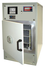
 Plasma Etch Inc of Carson City, NV, USA has launched the PE-100 low-cost plasma etching system for universities, small R&D laboratories and pilot production facilities.
The PE-100 provides a modestly sized vacuum chamber that accommodates up to 240” of process area capacity per run cycle. An RF power supply with matching network, vacuum pumping, and PLC-based process/vacuum controller with touch-screen programming is all included as a complete turn-key package. Any process developed on the PE-100 can be scaled up to Plasma Etch’s larger systems, as required by substrate size and throughput demands.
All Plasma Etch systems operate using a dry RF-induced ionized plasma process, enabling uniform removal of contaminants such as organics, coatings and metal oxides as well as providing a hydrophilic surface for adhesion of subsequent part processing. Applications include solar cells, MEMS, wafer-level packaging and other related semiconductor processes.
Search: Plasma etch Solar cells
Visit: www.plasmaetch.com